Microcontroller-Specific Details
Where the functions and data structures described in the CowPi Library and CowPi_stdio Library sections are applicable to any microcontroller that might be found on a Cow Pi board, the discussion in this section focuses on details that are particular to a specific microcontroller or family of microcontrollers. For each supported microcontroller, we discuss I/O registers and the CowPi library’s memory-mapped I/O data structures for them, we discuss interrupts (going beyond the CowPi library’s Pin Interrupts functions), and we also discuss some uses of the microcontroller’s timers.
ATmega328P (Arduino Nano, Arduino Uno R3)
Input/Output Register Descriptions
The ATmega328P microcontroller has the AVR instruction set’s original port-mapped input/output registers; however, it also has a much more extensive set of memory-mapped input/output registers. We recommend using the memory-mapped I/O registers and describe them here.
The tables below include each register’s address in the ATmega328P’s memory address space.
External Pins Input/Output
The ATmega328P microcontroller has three input/output ports accessible by external pins.
Each port has three registers, the PIN input register, the PORT output register, and the DDR data direction register used to set each pin as input or output.
Each pin is individually controlled by a particular bit in the port registers.
Table 6 shows these nine registers and their corresponding address offsets from the I/O base address.
You do not need to configure the pins’ directions for input or output; the cowpi_setup() function takes care of all necessary configuration.
Name |
Address |
Bit7 |
Bit6 |
Bit5 |
Bit4 |
Bit3 |
Bit2 |
Bit1 |
Bit0 |
|---|---|---|---|---|---|---|---|---|---|
PORTD
DDRD
PIND
|
0x2B
0x2A
0x29
|
PORTD7
DDRD7
PIND7
|
PORTD6
DDRD6
PIND6
|
PORTD5
DDRD5
PIND5
|
PORTD4
DDRD4
PIND4
|
PORTD3
DDRD3
PIND3
|
PORTD2
DDRD2
PIND2
|
PORTD1
DDRD1
PIND1
|
PORTD0
DDRD0
PIND0
|
PORTC
DDRC
PINC
|
0x28
0x27
0x26
|
PORTC7
DDRC7
PINC7
|
PORTC6
DDRC6
PINC6
|
PORTC5
DDRC5
PINC5
|
PORTC4
DDRC4
PINC4
|
PORTC3
DDRC3
PINC3
|
PORTC2
DDRC2
PINC2
|
PORTC1
DDRC1
PINC1
|
PORTC0
DDRC0
PINC0
|
PORTB
DDRB
PINB
|
0x25
0x24
0x23
|
PORTB7
DDRB7
PINB7
|
PORTB6
DDRB6
PINB6
|
PORTB5
DDRB5
PINB5
|
PORTB4
DDRB4
PINB4
|
PORTB3
DDRB3
PINB3
|
PORTB2
DDRB2
PINB2
|
PORTB1
DDRB1
PINB1
|
PORTB0
DDRB0
PINB0
|
Fig. 1–Fig. 4 show which bit in which port corresponds to each Arduino pin.
For example, pin D10 is labeled “PB2” indicating that it is part of port B and uses bit 2 in each of port B’s registers.
If D10 were an input pin, then we could determine the pin’s logic level by using a bitmask to examine PINB‘s bit 2.
On the other hand, if D10 were an output pin, then we could set the pin’s logic level to high or low by assigning a 1 or 0, respectively, to PORTB‘s bit 2, using the read/modify/write pattern.
Structure for Memory-Mapped Input/Output
The CowPi library provides data structures to access the memory-mapped I/O registers in a more readable form.
Specifically, the cowpi_ioport_t structure eliminates the need to remember which I/O port registers are used for output to peripherals and which are used for input from peripherals.
-
struct cowpi_ioport_t
Structure for the general-purpose I/O pins.
An array of these structures can be indexed using named constants (COWPI_PB, etc).
The ATmega328P’s three I/O ports are placed contiguously in the memory address space, which will allow us to create a pointer to the lowest-addressed port (0x23, per Table 6)
and then treat that pointer as an array of I/O ports.
Some named constants that we can use to index that array further eliminate the need to remember which port corresponds to each Arduino pin.
#define COWPI_PB  0                 //!< Index for arrays to access PINB/DDRB/PORTB and PCMSK0
#define D8_D13    0                 //!< Alias of COWPI_PB corresponding to pins D8-D13 on the Arduino Uno & Arduino Nano
#define COWPI_PC  1                 //!< Index for arrays to access PINC/DDRC/PORTC / PCMSK1
#define A0_A5     1                 //!< Alias of COWPI_PC for corresponding to pins D14-D19 (A0-A5) on the Arduino Uno & Arduino Nano
#define D14_D19   1                 //!< Alias of COWPI_PC for corresponding to pins D14-D19 (A0-A5) on the Arduino Uno & Arduino Nano
#define A0_A7     1                 //!< Alias of COWPI_PC for corresponding to pins D14-D19 (A0-A5) on the Arduino Uno & Arduino Nano
#define D14_D21   1                 //!< Alias of COWPI_PC for corresponding to pins D14-D19 (A0-A5) on the Arduino Uno & Arduino Nano
#define COWPI_PD  2                 //!< Index for arrays to access PIND/DDRD/PORTD and PCMSK2
#define D0_D7     2                 //!< Alias of COWPI_PD for corresponding to pins D0-D7 on the Arduino Uno & Arduino Nano
Tip
We recommend using D0_D7, D8_D13, and D14_D19.
Using our earlier hypotheticals:
If D10 were an input pin, then we could determine the pin’s logic level with C code similar to this:
1volatile cowpi_ioport_t *ioports = (cowpi_ioport_t *)(0x23); // an array of I/O ports
2uint8_t logic_level = ioports[D8_D13].input & (1 << (10-8));
In the first lines, we created our array of cowpi_ioport_t structures and assigned the array’s base address to 0x23.
Most likely, you would only need to do this once per program.
In the second line, we indexed the array using a named constant.
The convenient mapping of the Arduino’s pins to the ATMega328P’s I/O registers allows us to use named constants whose names help us remember which constant is appropriate for the pin we’re using.
After indexing the array, we select the input field because in this hypothetical, pin D10 is an input pin.
We use a bitmask so that we only capture the logic level of the pin we’re interested in.
Both 0x04 and 0b00000100 would be entirely suitable literal masks, and a mask created from a bitshift (i.e., (1 << 2)) is also appropriate.
Here we used (1 << (10-8)) because the convenient mapping of pins to registers allows us to create a mask from a bitshift without having to think about how many positions to shift – we simply subtracted the pin number (10) from the lowest-number pin in this bank (8).
Of course, in this example, logic_level would take on either a zero or non-zero value, which is fine for most applications.
If logic_level must take on either zero or one, then you could either shift the bits:
3uint8_t logic_level = (ioports[D8_D13].input & (1 << (10-8))) >> (1 >> (10-8));
or double-negate:
3uint8_t logic_level = !!(ioports[D8_D13].input & (1 << (10-8)));
On the other hand, if D10 were an output pin, then we could set the pin’s logic level with C code similar to this:
1volatile cowpi_ioport_t *ioports = (cowpi_ioport_t *)(0x23); // an array of I/O ports
2// to clear pin 10 to a 0:
3ioports[D8_D13].output &= ~(1 << (10-8));
4// to set pin 10 to a 1:
5ioports[D8_D13].output |= 1 << (10-8);
This code uses the read/modify/write pattern: Obtain the existing output values for the relevant bank of pins, then create a bit vector that can be used to set 0 or 1 in the specific bit while preserving all of the other pins’ output values, and then finally assign the resulting bit vector to the bank’s output register. If the new logic level is in a variable and you don’t know whether you’re assigning a 0 or a 1, a good choice would be to clear the relevant bit to 0 and then use a bitwise OR to assign the appropriate value to the specific bit:
3uint8_t logic_level = ... // assume logic_level is strictly 0 or 1
4ioports[D8_D13].output = (ioports[D8_D13].output & ~(1 << (10-8))) | (logic_level << (10-8));
Mapping Input/Output Devices to I/O Port Array
The Structure for Memory-Mapped Input/Output Section describes the I/O ports, a structure definition, and named constants that can be used to access the inputs and outputs attached to the Arduino’s pins. Fig. 1 & Fig. 3 show which input/output devices are attached to the various Arduino pins when SPI is used to communicate with the display module. Combining this information, we arrive at the mapping in Table 7 that is suitable for the Cow Pi mk1e, and for the Cow Pi mk3a & 3b when configured for SPI.
Array Element |
Field |
Bit7 |
Bit6 |
Bit5 |
Bit4 |
Bit3 |
Bit2 |
Bit1 |
Bit0 |
|---|---|---|---|---|---|---|---|---|---|
|
.input.output |
—
Keypad
Row *
|
—
Keypad
Row 7
|
—
Keypad
Row 4
|
—
Keypad
Row 1
|
—
—
|
—
—
|
—
—
|
—
—
|
|
.input.output |
—
—
|
—
—
|
— SPI
Clock Pin
& LeftLED
|
—
Right
LED
|
— SPI
Data
Pin
|
— SPI
Latch
Pin
|
Right
Button
—
|
Left
Button
—
|
|
.input.output |
—
—
|
—
—
|
Left
Switch
—
|
Right
Switch
—
|
Keypad
Col A
—
|
Keypad
Col 3
—
|
Keypad
Col 2
—
|
Keypad
Col 1
—
|
Similarly, by combining the information in the Structure for Memory-Mapped Input/Output Section with the information in Fig. 2 & Fig. 4, we arrive at the mapping in Table 8 that is suitable for the Cow Pi mk1f, and for the Cow Pi mk3a & 3b when configured for I2C.
Array Element |
Field |
Bit7 |
Bit6 |
Bit5 |
Bit4 |
Bit3 |
Bit2 |
Bit1 |
Bit0 |
|---|---|---|---|---|---|---|---|---|---|
|
.input.output |
—
Keypad
Row *
|
—
Keypad
Row 7
|
—
Keypad
Row 4
|
—
Keypad
Row 1
|
—
—
|
—
—
|
—
—
|
—
—
|
|
.input.output |
—
—
|
—
—
|
—
Left
LED
|
—
Right
LED
|
Left
Switch
—
|
Right
Switch
—
|
Right
Button
—
|
Left
Button
—
|
|
.input.output |
—
—
|
—
—
|
controlled by
I2C for
display module
|
Keypad
Col A
—
|
Keypad
Col 3
—
|
Keypad
Col 2
—
|
Keypad
Col 1
—
|
|
Serial-Parallel Interface
The ATmega328P uses three registers for SPI:
SPCRThe SPI Control Register is used to configure the SPI hardware.
SPSRThe SPI Status Register is used to indicate the status of a data transfer.
SPDRThe SPI Data Register is used to transfer data to and from an SPI peripheral device.
The SPI hardware has four modes of operation: controller output/peripheral input and controller input/peripheral output as the controller; and controller output/peripheral input and controller input/peripheral output as the peripheral.[1] In the Cow Pi’s typical usage, the controller output/peripheral input mode will be used to drive the display module. For this reason, the discussion in this datasheet will focus on the controller output/peripheral input mode.
In general, the nature of SPI allows for uses other than the display module without compromising the ability to work with the display module;
however, the limited number of ATmega328P data pins would make this challenging.
If you choose to expand the Cow Pi in such a manner that controller input/peripheral output is necessary, see Chapter 18 of the ATmega328P datasheet for details.
You will need to write a custom cowpi_max7219_send() function – or at least a custom cowpi_spi_finalize function – that does not disable the SPI hardware upon completion.
We strongly advise against using the ATmega328P as a peripheral while it is in the Cow Pi circuit.
Structure for Memory-Mapped Input/Output
The CowPi library provides data structures to access the memory-mapped I/O registers in a more readable form.
Specifically, the cowpi_spi_t structure provides meaningfully-named fields in place of the 4-letter register names.
-
struct cowpi_spi_t
Structure for the SPI hardware.
Unlike the I/O registers for the external pins, you will not have an array of cowpi_spi_t structures; you’ll have just the one.
Create a pointer to a cowpi_spi_t structure that points to the lowest-addressed register (TWBR, 0x4C, per Table 9).
For example, if we wanted to determine if a serial transfer had been completed, and then enable the SPI hardware as a controller with a 1MHz bit rate, then we could do so with C code similar to this:
1volatile cowpi_spi_t *spi = (cowpi_spi_t *)(0x4C);
2uint8_t status = spi->status & 0x80; // mask-off the irrelevant bits
3spi->control = (1 << 6) | (1 << 4) | (1 << 0);  // Enable bit | Controller bit | Prescaler 16
You may have noticed that this code does not use the read/modify/write pattern. Because of the particular uses of the control bits, you may find it easier to explicitly assign each control bit value afresh, rather than modify the pre-existing values.
SPI Register Bits
Table 9 identifies the particular bits in each of the SPI registers.
Register Name |
Address |
Bit7 |
Bit6 |
Bit5 |
Bit4 |
Bit3 |
Bit2 |
Bit1 |
Bit0 |
|---|---|---|---|---|---|---|---|---|---|
Data Register
TSPR
|
0x4E |
MSB |
… |
… |
… |
… |
… |
… |
LSB |
Status Register
SPSR
|
0x4D |
SPIF |
WCOL |
— |
— |
— |
— |
TWPS1 |
SPI2X |
Control Register
SPCR
|
0x4C |
SPIE |
SPE |
DORD |
CTLR |
CPOL |
CPHA |
SPR1 |
SPR0 |
The CowPi_stdio library configures the SPI hardware to transmit at 1Mbps. In this section we focus on the needs of the application programmer. If you need information about the setting the bit rate, or configuring the peripheral address and address mask, see Section 18.5 of the ATmega328P datasheet for the bit descriptions, and Chapter 18 generally for the bits’ uses.
Data Bits
The eight data bits are straight-forward.
When in controller output/peripheral input mode, place the byte that needs to be transmitted into the SPI Data Register (or the data field of a cowpi_spi_t variable);
there is generally no need to use the distinct bits.
Similarly, when in controller input/peripheral output mode, the last byte sent by the transmitter can be found in the SPI Data Register.
Status Bits
There are two bits in the SPI Status Register that allow a program to learn when it is safe to control the hardware, and one that is actually a control bit.
- Bit 7, SPI Interrupt Flag
The SPI hardware sets this bit to a 1 when it has finished its last operation and the program can safely write to the data register. The program clears the flag by reading from the SPI Status Register when the bit is 1. and then writing to the SPI Data Register; this causes the bit to become 0. Once the bit is 0, the program should not write to the data registers until it is 1 again. You can create a busy-wait loop that blocks the program while the bit is 0.
Alternatively, if SPI interrupts are enabled then you can create an interrupt handler that updates the data register only when it is safe to do so. The
cowpi_spi_initialize_hardware()function initially disables SPI interrupts; you must explicitly enable SPI interrupts in a custom function if you intend to use them.- Bit 6, Write Collision Flag
If a program writes to the data register while the TWI Interrupt Flag (bit 7) is 0, a data collision will occur, and this bit will become 1. If you only use controller output/peripheral input mode and you always use a busy-wait loop that blocks the program while the SPI Interrupt Flag is 0, then the Write Collision Flag should never become 1.
- Bit 0, SPI Double Speed Bit
Setting this bit causes the clock rate to be double what it otherwise would be at.
Control Bits
There are eight bits that are used to configure teh SPI hardware
- Bit 7, SPI Interrupt Enable
Causes an SPI interrupt to fire whenever the SPI Interrupt Flag becomes 1.
- Bit 6, SPI Enable
When this bit is 1, the SPI hardware controls both SPI data pins and the SPI clock pin. Only one of the SPI data pins is used by the Cow Pi as a data pin; the other is used for the right LED, and the clock pin is used for the left LED. For this reason,
cowpi_spi_initialize_hardware()enables the SPI hardware, andcowpi_spi_finalize_hardware()disables the SPI hardware.- Bit 5, Data Order
If this bit is 0 then the most significant bit is transmitted first; if this bit is 1 then the least significant bit is transmitted first.
- Bit 4, Controller/Peripheral Select
The ATmega328P acts as the SPI controller when this bit is 1, and as a SPI peripheral when this bit is 0.
- Bit 3, Clock Polarity
- Bit 2, Clock Phase
Orthogonal to the controller output/peripheral input and controller input/peripheral output modes, there are another four modes based on the clock’s attributes. See Section 18.4 of the ATmega328P datasheet.
- Bit 1, SPI Clock Rate Select 1
- Bit 0, SPI CLock Rate Select 0
The clock rate is determined by a prescaler applied to the system clock. See Table 18.5 of the ATmega328P datasheet.
Controller Output/Peripheral Input Sequence
The typical SPI controller output/peripheral input sequence is:
if necessary, enabling the SPI hardware
signaling the peripheral to receive data by setting the chip select pin to 0
transmitting one or more data bytes
signaling the peripheral to latch the data into its permanent register by setting the chip select pin to 1
if necessary, disabling the SPI hardware
After each transmission, the program should busy-wait until the SPI Interrupt Flag has been set (bit 7 of SPSR or the status field of a cowpi_spi_t variable).
The pseudocode for this sequence is:
1(* assume variable i2c is a reference to a cowpi_i2c_t structure *)
2(* assume variable bit_order indicates whether the peripheral expects MSB first (0) or LSB first (1) *)
3(* assume variable select_pin is an integer identifying the chip select pin *)
if necessary, enable the SPI hardware
5        (* Enable SPI, data order, Controller, set clock rate 1MHz *)
6spi->control := bitwise_or((1 << 6), (bit_order << 5), (1 << 4), (1 << 0))
transmit one or more data bytes:
 8        (* signal the peripheral to receive data *)
 9set_pin(select_pin, 0);
10        (* send the data that the peripheral needs *)
11for each byte of data do
12    spi->data := data_byte
13    busy_wait_while(bit 7 of i2c->status = 0)
14        (* signal the peripheral to latch data *)
15set_pin(select_pin, 1);
if necessary, enable the SPI hardware
17        (* Disable SPI *)
18spi->control := 0
Tip
The for each expression in the pseudocode should be understood to be the mathematical  operator.
If there are several bytes that are handled identically, then writing a loop probably makes sense.
On the other hand, if there are a small number of bytes, each of which must be handled differently,
then it probably makes more sense to write straight-line code.
operator.
If there are several bytes that are handled identically, then writing a loop probably makes sense.
On the other hand, if there are a small number of bytes, each of which must be handled differently,
then it probably makes more sense to write straight-line code.
Attention
The specific data byte sequence to be transmitted is described in the HD44780-driven LCD Character Display portion of the Output Devices Section.
Inter-Integrated Circuit Protocol
The ATmega328P uses six registers for I2C. In this datasheet, we use the conventional terms “Inter-Integrated Circuit,” or I2C; however, the ATmega328P datasheet uses the terms “Two Wire Interface,” or TWI, to describe the I2C protocol. We mention this because the six registers, and the bits contained therein, have names derived from “TWI.”
The six registers are:
TWBRThe TWI Bit Rate Register, along with the prescaler bits in TWSI, is used to set the transmission bit rate. You do not need to configure the bit rate; the CowPi_stdio library takes care of all necessary configuration to set the bit rate to 100kHz.
TWCRThe TWI Control Register controls the operation of the I2C hardware. The particular bits are described in the Control and Data Bits Section.
TWSRThe TWI Status Register is principally used to reflect the status of the I2C hardware and the I2C serial bus. Bits 1..0 are define the prescaler that, along with TWBR, set the transmission bit rate. The remaining bits are described in the Control and Data Bits Section.
TWDRThe TWI Data Register contains either the next byte to transmit or the last byte received, depending on the current mode of operation. The particular bits are described in the Control and Data Bits Section.
TWARThe TWI Address Register sets the microcontroller’s address when the I2C hardware is configured to act as a peripheral. Under normal Cow Pi operation, TWAR is unused.
TWAMRThe TWI Address Mask Register instructs the I2C hardware, when configured to act as a peripheral, to ignore particular bits when determining whether this microcontroller is being addressed. Under normal Cow Pi operation, TWAMR is unused.
The I2C hardware has four modes of operation: controller transmitter, controller receiver, peripheral transmitter, and peripheral receiver.[1] In the Cow Pi’s typical usage, the controller transmitter mode will be used to drive the display module. For this reason, the discussion in this datasheet will focus on the controller transmitter mode.
The nature of I2C allows for uses other than the display module without compromising the ability to work with the display module. If you choose to expand the Cow Pi in such a manner that other I2C modes are necessary, see Section 21.7 of the ATmega328P datasheet for details.
We strongly advise against using the ATmega328P as a peripheral while it is in the Cow Pi circuit.
Structure for Memory-Mapped Input/Output
The CowPi library provides data structures to access the memory-mapped I/O registers in a more readable form.
Specifically, the cowpi_i2c_t structure provides meaningfully-named fields in place of the 4–5-letter register names.
-
struct cowpi_i2c_t
Structure for the TWI (aka I2C, IIC) hardware.
Public Members
-
uint8_t bit_rate
TWI bit rate register, works in concert with status register (TWBR)
-
uint8_t status
TWI status register (TWSR)
-
uint8_t address
TWI peripheral address register (TWAR)
-
uint8_t data
TWI data register (TWBB)
-
uint8_t control
TWI control register(TWCR)
-
uint8_t peripheral_address_mask
TWI peripheral address mask register (TWAMR)
-
uint8_t bit_rate
Unlike the I/O registers for the external pins, you will not have an array of cowpi_i2c_t structures; you’ll have just the one.
Create a pointer to a cowpi_i2c_t structure that points to the lowest-addressed register (TWBR, 0xB8, per Table 10).
For example, if we wanted to determine if a status had been set, and then set the TWI Enable bit (TWEN), then we could do so with C code similar to this:
1volatile cowpi_i2c_t *i2c = (cowpi_i2c_t *)(0xB8);
2uint8_t status = i2c->status & 0xF8; // mask-off the irrelevant bits
3i2c->control = 0x4; // Set the Enable bit
You may have noticed that this code does not use the read/modify/write pattern. Because of the particular uses of the control bits, you may find it easier to explicitly assign each control bit value afresh, rather than modify the pre-existing values.
Control and Data Bits
Table 10 identifies the particular bits in each of the I2C registers.
Register Name |
Address |
Bit7 |
Bit6 |
Bit5 |
Bit4 |
Bit3 |
Bit2 |
Bit1 |
Bit0 |
|---|---|---|---|---|---|---|---|---|---|
Peripheral Address Mask Register
TWAMR
|
0xBD |
TWAM6 |
TWAM5 |
TWAM4 |
TWAM3 |
TWAM2 |
TWAM1 |
TWAM0 |
— |
Control Register
TWCR
|
0xBC |
TWINT |
TWEA |
TWSTA |
TWSTO |
TWWC |
TWEN |
— |
TWIE |
Data Register
TWDR
|
0xBB |
TWD7 |
TWD6 |
TWD5 |
TWD4 |
TWD3 |
TWD2 |
TWD1 |
TWD0 |
Peripheral Address Register
TWAR
|
0xBA |
TWA6 |
TWA5 |
TWA4 |
TWA3 |
TWA2 |
TWA1 |
TWA0 |
TWGCE |
Status Register
TWSR
|
0xB9 |
TWS7 |
TWS6 |
TWS5 |
TWS4 |
TWS3 |
— |
TWPS1 |
TWPS0 |
Bit Rate Register
TWBR
|
0xB8 |
TWBR7 |
TWBR6 |
TWBR5 |
TWBR4 |
TWBR3 |
TWBR2 |
TWBR1 |
TWBR0 |
The CowPi_stdio library configures the I2C hardware to transmit at 100kbps. In this section we focus on the needs of the application programmer and shall describe only the control and data bits. If you need information about the setting the bit rate, or configuring the peripheral address and address mask, see Section 21.9 of the ATmega328P datasheet for the bit descriptions, and Chapter 21 generally for the bits’ uses.
Data Bits
The eight data bits are straight-forward.
When in controller transmitter mode, place the byte that needs to be transmitted into the TWI Data Register (or the data field of a cowpi_i2c_t variable);
there is generally no need to use the distinct bits.
Similarly, when in controller receiver mode, the last byte sent by the transmitter can be found in the TWI Data Register.
Control Bits
There are seven bits that either allow a program to control the I2C hardware or to learn when it is safe to control the hardware.
- Bit 7, TWI Interrupt Flag
The I2C hardware sets this bit to a 1 when it has finished with its last operation and the program can safely write to the data and status registers. Perhaps counterintuitively, the program clears the flag by writing a 1 to this bit; this causes the bit to become 0. Once the bit is 0, the program should not write to the status or data registers until it is 1 again. You can create a busy-wait loop that blocks the program while the bit is 0.
Alternatively, if TWI interrupts are enabled then you can create an interrupt handler that updates the data and status registers only when it is safe to do so (and then clears this bit). The
cowpi_i2c_initialize_hardware()function initially disables TWI interrupts; you must explicitly enable TWI interrupts in a custom function if you intend to use them.- Bit 6, TWI Enable Acknowledge Bit
When the program has set this bit to 1, it instructs the I2C hardware to generate an ACK signal at the appropriate times when in controller receiver, peripheral transmitter, or peripheral receiver modes.
- Bit 5, TWI Start Condition Bit
As part of the I2C protocol, the controller must send a “Start Bit” when it needs to control the I2C bus. A program can instruct the I2C hardware to claim control of the bus (or wait until it can do so) by writing a 1 to this bit and also to bit 7 (the TWI Interrupt Flag bit). When the controller has control of the bus, the TWI Interrupt Flag (bit 7) will become 1.
- Bit 4, TWI Stop Condition Bit
As part of the I2C protocol, the controller must send a “Stop Bit” when it no longer needs to control the I2C bus. A program can instruct the I2C hardware to release control of the bus by writing a 1 to this bit and also to bit 7 (the TWI Interrupt Flag bit).
- Bit 3, TWI Write Collision Flag
If a program writes to the data register while the TWI Interrupt Flag (bit 7) is 0, a data collision will occur, and this bit will become 1. If you only use controller transmitter mode and you always use a busy-wait loop that blocks the program while the TWI Interrupt Flag is 0, then the TWI Write Collision Flag should never become 1.
- Bit 2, TWI Enable Bit
This bit must be a 1 at all times for the I2C hardware to work, and the function initially sets it to 1; if, as recommended in the Structure for Memory-Mapped Input/Output Section, you explicitly assign each bit value instead of using the read/modify/write pattern, then be sure that you always assign a 1 to this bit.
- Bit 0, TWI Interrupt Enable
If this bit is 1, then TWI interrupt requests will be activated whenever appropriate. If this bit is 0, then TWI interrupt requests will not be activated. T he function initially disables TWI interrupts.
Controller Transmitter Sequence
Generally speaking, the I2C controller transmitter sequence consists of:
contacting the peripheral by transmitting a start bit followed by the desired peripheral’s address (plus a mode bit)
transmitting one or more data bytes
transmitting a stop bit
After each transmission, the program should busy-wait until the TWI Interrupt Flag has been set (bit 7 of TWCR or the control field of a cowpi_i2c_t variable).
After the busy-wait terminates, the I2C status can be checked (bits 7..3 of TWSR or the status field of a cowpi_i2c_t variable) to determine whether there were any errors.
Table 21-3 of the ATmega328P datasheet specifies what the status bits should be after each transmission.
The pseudocode for this sequence is:
1(* assume variable i2c is a reference to a cowpi_i2c_t structure *)
2
3        (* every assignment to i2c->control needs to:
4           write a 1 to bit 7 to clear the interrupt flag, and
5           write a 1 to bit 2 to keep I2C enabled *)
6control_bits := bitwise_or((1 << 7), (1 << 2))
contact the peripheral by transmitting a start bit followed by the desired peripheral’s address (plus a mode bit)
 8        (* send the start bit by writing a 1 to bit 5 of i2c->control *)
 9i2c->control := bitwise_or(control_bits, (1 << 5))
10
11        (* wait until operation finishes *)
12busy_wait_while(bit 7 of i2c->control = 0)
13
14(* if controller now controls the I2C bus, then bitwise_and(i2c->status, 0xF8) is 0x08 *)
15
16        (* when sending the peripheral's address, it should be in the data
17           register's bits 7..1 -- bit 0 should be 0 for controller-transmitter *)
18i2c->data := (peripheral_address << 1)
19
20        (* send contents of data register *)
21i2c->control := control_bits
22busy_wait_while(bit 7 of i2c->control = 0)
23
24(* if peripheral sent ACK, then bitwise_and(i2c->status, 0xF8) is 0x18 *)
transmit one or more data bytes
26        (* send the data that the peripheral needs *)
27for each byte of data do
28    i2c->data := data_byte
29    i2c->control := control_bits
30    busy_wait_while(bit 7 of i2c->control = 0)
31
32    (* if peripheral sent ACK, then bitwise_and(i2c->status, 0xF8) is 0x28 *)
transmit a stop bit
33        (* send the stop bit by writing a 1 to bit 4 of i2c.control *)
34i2c->control := bitwise_or(control_bits, (1 << 4))
35        (* unlike the START, address, and data transmissions, the STOP transmission
36           does not set the TWINT bit when finished, but we shouldn't start another
37           transmission while the STOP transmission is in-progress -- so we shall
38           delay at least (8 bits / 100,000 bits per second = 80 microseconds) *)
39timed_wait(80 microseconds or longer)
Tip
The for each expression in the pseudocode should be understood to be the mathematical operator.
If there are several bytes that are handled identically, then writing a loop probably makes sense.
On the other hand, if there are a small number of bytes, each of which must be handled differently,
then it probably makes more sense to write straight-line code.
Attention
The specific data byte sequence to be transmitted is described in the HD44780-driven LCD Character Display portion of the Output Devices Section.
Interrupts
Most interrupts on the ATmega328P are handled by creating an interrupt service routine (ISR) using AVR-libc’s ISR() macro.
Pin change interrupts can be handled either by using the ISR() macro or by using the Cow Pi library’s cowpi_register_pin_ISR() function.
External interrupts can be handled either by using the ISR() macro or by using the Arduino attachInterrupt() function to register an interrupt handler.
Registering Interrupt Service Routines using the ISR() Macro
To create an interrupt service routine, write this code that looks like a function, outside of any other function:
ISR(vector) {
    ...
}
where vector is one of the vectors listed in the AVR-libc’s interrupts documentation
(look in the table rows that have “ATmega328P” in the “Applicable for Device” cell).
Replace ... with the code that should execute whenever the timer interrupt occurs.
You want to keep your ISR short, no more than a few lines of code.
If anything more elaborate needs to happen, code in your function (or a function called by ) can do that based on changes made from within your ISR.
Any necessary configuration to establish the conditions under which the ISR will be invoked, typically through the use of memory-mapped I/O registers, will need to occur either in the setup() function or in a helper function called by setup().
Registering Pin Change Interrupt Handlers using cowpi_register_pin_ISR()
The ATmega328P has two types of interrupts that are based on changes detected at the pins, Pin Change Interrupts and External Interrupts.
Pin Change Interrupts are generally less flexible in that an interrupt would be fired for any changes,
and when using the ISR() macro, all pins on the same I/O bank must use the same ISR.
On the other hand, pin change interrupts are more flexible in that they can be triggered by changes on any of the digital pins.
The CowPi library’s cowpi_register_pin_ISR() function abstracts away the configuration details and also allows pins to have a different ISR than other pins on the same I/O bank.
To handle an interrupt, first write a function, such as handle_buttonpress() or handle_keypress().
This function must not have any parameters, and its return type must be void.
Then, in the setup() function (or in one of its helper functions), register the interrupt with this code:
cowpi_register_pin_ISR(1L << pin_number, interrupt_handler_name);
or
cowpi_register_pin_ISR((1L << first_pin_number) | (1L << second_pin_number) | (1L << et_cetera), interrupt_handler_name);
This will configure all of the necessary registers to call the function whenever the input value on the pin pin_number (or on the pins first_pin_number, second_pin_number, …, et_cetera) goes from 0 to 1 or from 1 to 0.
The first argument is a bit vector that identifies which pin(s) are to be associated with the ISR:
if bit n is a 1, then pin n will be associated with the ISR.
Tip
If the pin number is greater than 15, be sure to use 1L instead of 1 to prevent truncation during the bit shift.
As with ISRs registered with the macro, you want to keep your interrupt handler short. See the CowPi library’s pin_interrupts example for demonstrations.
Registering External Interrupt Handlers using attachInterrupt()
External Interrupts can also be manually configured and handled through the ISR() macro.
Just as the CowPi library’s cowpi_register_pin_ISR() function abstracts away the configuration details for pin change interrupts,
the Arduino attachInterrupt() function abstracts away the configuration details for external interrupts.
While external interrupts on the ATmega328P are limited to only two pins (digital pins D2 & D3), their triggering conditions can be tailored.
To handle an interrupt, first write a function, such as handle_buttonpress() or handle_keypress().
This function must not have any parameters, and its return type must be void.
Then, in the setup() function (or in one of its helper functions), register the interrupt with this code:
attachInterrupt(digitalPinToInterrupt(pin_number), interrupt_handler_name, mode);
This will configure all of the necessary registers to call the function whenever the input value on the pin pin_number satisfies the mode. The mode is one of:
- LOW
to trigger the interrupt whenever the pin is 0
- RISING
to trigger the interrupt whenever the pin goes from 0 to 1
- FALLING
to trigger the interrupt whenever the pin goes from 1 to 0
- CHANGE
to trigger the interrupt whenever the pin rises or falls
As with ISRs registered with the macro, you want to keep your interrupt handler short.
Timers
The ATmega328P used by the Arduino in the Cow Pi has three timers. As with the other I/O registers, the registers used by these timers are mapped into the data memory address space.
Structures for Memory-Mapped Timer Registers
The CowPi library provides data structures for both 8-bit and 16-bit timers, allowing access to the memory-mapped timer registers in a more readable form.
-
struct cowpi_timer8bit_t
Structure for 8-bit timer/counter (TIMER0 or TIMER1).
The timer/counter interrupt mask register (TIMSKx) and the timer/counter interrupt flag register (TIFRx) are not part of this structure. Neither are the asynchronous status register (ASSR) nor the general timer/counter control register (GTCCR).
-
struct cowpi_timer16bit_t
Structure for 16-bit timer/counter (TIMER1).
The timer/counter interrupt mask register (TIMSKx) and the timer/counter interrupt flag register (TIFRx) are not part of this structure. Does not include the general timer/counter control register (GTCCR).
Public Members
-
uint32_t control
Timer/counter control registers A, B, & C; register A is the low-order byte (Reserved TCCRxC TCCRxB TCCRxA)
-
uint16_t counter
Timer/counter register (TCNTxH TCNTxL, aka TCNTx)
-
uint16_t capture
Input capture register (ICRxH ICRxL, aka ICRx)
-
uint16_t compareA
Output compare register A (OCRxAH OCRxAL, aka OCRxA)
-
uint16_t compareB
Output compare register B (OCRxBH OCRxBL, aka OCRxB)
-
uint32_t control
The ATmega328P’s TIMER0 and TIMER2 are 8-bit timers, and TIMER1 is a 16-bit timer.
Important
Even though TIMER0 and TIMER2 are both 8-bit timers and make use of the same cowpi_timer8bit_t structure definition, the interpretation of the bits in their fields is subtly different.
Be sure to use the correct tables when configuring the timers.
Caution
The timers have uses which may not be immediately obvious.
The most critical of these is that TIMER0 is used for the pseudo-clock that allows the Arduino millis() function to report the number of milliseconds since power-up.
The CowPi_stdio library also uses TIMER0 for some display modules.
While you can safely configure and handle comparison interrupts that do not reset the timer’s counter,
you should not change TIMER0’s period, reset TIMER0’s counter, nor register an ISR for TIMER0_OVF0_vect nor TIMER0_COMPB_vect unless you are willing to accept the adverse impact on millis() and the timer-based display modules, and any code that depends on millis().
The five fields in the structures are:
controlThe concatenation of the timer’s two (TIMER0, TIMER2) or three (TIMER1) control registers
counterThe 8-bit (TIMER0, TIMER2) or 16-bit (TIMER1) value that increments by one in each timer period
captureStores the counter’s value at the exact moment that an input capture event occurs (TIMER1 only)
compareAThe counter value at which a
TIMERn_COMPA_vectinterrupt should be triggered, where n is the timer numbercompareBThe counter value at which a
TIMERn_COMPB_vectinterrupt should be triggered, where n is the timer number
Configuring the Timer Period
The timers have a few different waveform generation modes. To understand the available waveform generation modes, see the ATmega328P datasheet; specifically, see Section 14.7 (TIMER0), Section 15.9 (TIMER1), or Section 17.7 (TIMER2).
For typical Cow Pi usage, we anticipate only Normal mode and Clear Timer on Compare (CTC) mode will be used.
For these modes, you can configure the timer by setting the appropriate waveform generation mode (WGM) bits and clock source (CS) bits in the timer structure’s control field,
and possibly a value in one of the compareX fields.
In this section, we describe how to arrive at the prescaler value that will be used to determine the CS bits and the comparison value if one is needed. In the sections for Configuring TIMER0, Configuring TIMER1, and Configuring TIMER2, we describe how to determine the WGM and CS bits. Finally, in the Timer Interrupts section, we describe how to enable the appropriate timer interrupt(s).
Normal Mode
In a timer’s Normal mode, it will increment its counter to the maximum value representable by its counter, and then overflow to zero, possibly generating a timer overflow interrupt in the process. You can adjust the rate at which its counter increments using a prescaler that is applied to the system clock’s period. Because the number of increments is fixed, a timer has only 5 or 7 possible periods without introducing an external timer source.
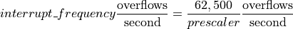
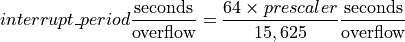
You can determine the interrupt frequency:

For TIMER0 and TIMER2, this reduces to
For TIMER1, this reduces to

The possible prescaler values are
- TIMER0:
1, 8, 64, 256, 1024
- TIMER1:
1, 8, 64, 256, 1024
- TIMER2:
1, 8, 32, 64, 128, 256, 1024
If you prefer to determine the interrupt period, it is straight-forward to determine that for TIMER0 and TIMER 2:
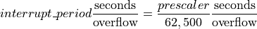
and for TIMER1:
You can configure an an interrupt to fire whenever a timer overflows.
For example, the Arduino core library sets TIMER0’s prescaler to 64, and so TIMER0 overflows every 1.024ms.
The Arduino core library also configures a timer overflow interrupt for TIMER0, and its ISR updates the pseudo-clock used by millis() every 1.024ms.
For each timer, you can also configure up to two comparison interrupts that fire whenever the timer reaches a particular value. All interrupts using the same timer have the same interrupt period. For example, the CowPi_stdio library registered a comparison interrupt for TIMER0 to support some display modules. We chose a comparison value of 0x40 since that leaves ample time for the pseudo-clock update to finish and also leaves plenty of time for another comparison ISR if you choose to configure another comparison interrupt on TIMER0.
Clear Timer on Compare Mode
In other timer modes, including Clear Timer on Compare (CTC) mode, you have a much wider range of possible intervals between interrupts available to you, which you can obtain by setting both a prescaler and a comparison value.
Once you know the desired timer period between timer interrupts, you need to determine the comparison value and the timer prescaler that will realize this timer period. You will probably arrive at the comparison value by trying each prescaler until you find a satisfying pair of values.

or, equivalently:

where:
- 16,000,000 Hz
is the system clock frequency (the inverse of the clock period).
- comparison_value
is how the number of “timer” beats between interrupts. You will notice that Normal mode’s equations are a special case of those presented here, in which comparison_value is
 .
You will subtract one from comparison_value and place in one of the timer’s
.
You will subtract one from comparison_value and place in one of the timer’s compareregisters for a comparison-based timer interrupt. This can be any possible value of an unsigned 16-bit integer for TIMER1, or any possible value of an unsigned 8-bit integer for TIMER0 and TIMER2.- prescaler
is a multiplier applied to the clock period to adjust the time between counter increments (“beats”). Possible values are
- TIMER0:
1, 8, 64, 256, 1024
- TIMER1:
1, 8, 64, 256, 1024
- TIMER2:
1, 8, 32, 64, 128, 256, 1024
- interrupt_frequency
is how often you want a timer interrupt (the inverse of the interrupt period).
- interrupt_period
is the time between timer interrupts (the inverse of the interrupt frequency).
You may have to iterate on your design until you arrive at one that works with the constraints of that equation’s terms for whichever timer you choose to use.
Note
If you cannot arrive at an integer comparison value for the exact interrupt period, then determine which combination of prescaler and comparison value produces the least error.
If you cannot generate a timer period great enough for your needs, then
find a comparison value and a prescaler that yield a timer period that is an integer factor of your actual desired period.
Then introduce a counter variable in your ISR that increments each time the ISR is invoked,
and when it reaches a particular value (the value at which  ) then take the appropriate action.
Based on the prescaler and comparison value you chose, use the tables below to configure the timer registers.
Configuring TIMER0
Caution
TIMER0 is used by the Arduino Core to track time since power-up.
The Arduino Core configures TIMER0 for “Normal” mode with a prescaler of 64, generating a timer overflow interrupt every 1.024ms. While it is perfectly safe to set up comparison interrupts using TIMER0, DO NOT change TIMER0’s Waveform Generation Mode or Clock Select bits, nor register an ISR for ``TIMER0_OVF_vect``, if your code relies upon the Arduino core to track time.
We also recommend against registering an ISR for TIMER0_COMPB_vect, as this interrupt vector is used by the CowPi_stdio library for timer-based display modules.
Table 11 shows the mapping of TIMER0’s registers to the cowpi_timer8bit_t struct.
Creating a pointer to TIMER0’s memory-mapped registers is as simple as:
1volatile cowpi_timer8bit_t *timer = (cowpi_timer8bit_t *)(0x44);
Having creating that pointer, you can access the registers using the cowpi_timer8bit_t‘s fields.
Name |
Address |
|
||||||||
|---|---|---|---|---|---|---|---|---|---|---|
OCR0B |
0x48 |
Bit7 … Bit0 |
||||||||
Comparison Value “B” |
||||||||||
OCR0A |
0x47 |
Bit7 … Bit0 |
||||||||
Comparison Value “A” |
||||||||||
TCNT0 |
0x46 |
Bit7 … Bit0 |
||||||||
Timer Counter Value |
||||||||||
TCCR0A |
0x44 |
Bit15 |
Bit14 |
Bit13 |
Bit12 |
Bit11 |
Bit10 |
Bit9 |
Bit8 |
|
FOC0A |
FOC0B |
— |
— |
WGM02 |
CS02 |
CS01 |
CS00 |
|||
Bit7 |
Bit6 |
Bit5 |
Bit4 |
Bit3 |
Bit2 |
Bit1 |
Bit0 |
|||
COM0A1 |
COM0A0 |
COM0B1 |
COM0B0 |
— |
— |
WGM01 |
WGM00 |
|||
The two comparison values, which you can set, are continuously compared to the timer’s counter value.
A comparison match can be used to generate an output compare interrupt (TIMER0_COMPA_vect or TIMER0_COMPB_vect).
The timer’s counter value can be read from or written to by your program.
Polling the counter value is a notional use case, but configuring an interrupt would be more appropriate.
Assigning a value, such as 0, to the counter would be a mechanism to reset its counter to a known value.
Among the bits in the control field (the TCCR0A & TCCR0B registers), most can be left as 0.
If you believe that you need to set custom “Force Output Compare” or “Compare Output Mode” bits, then consult the ATmega328P datasheet, Section 14.9.
Under typical Cow Pi usage, you should only need to set the “Waveform Generation Mode” and “Clock Select” bits.
Using the prescaler that you determined above, you should assign the CS00, CS01, and CS02 bits using Table 12.
CS02 |
CS01 |
CS00 |
Description |
|---|---|---|---|
0 |
0 |
0 |
No clock source (Timer/Counter stopped) |
0 |
0 |
1 |
|
0 |
1 |
0 |
|
0 |
1 |
1 |
|
1 |
0 |
0 |
|
1 |
0 |
1 |
|
 (prescaler 1)
 (prescaler 8)
 (prescaler 64)
 (prescaler 256)
 (prescaler 1024)
The Waveform Generation Bits are used to set the Timer/Counter mode of operation.
There are two modes most useful for typical Cow Pi usage.
The first is “Normal” mode, in which the counter increases monotonically until it reaches the greatest possible representable value and then overflows to 0.
The other mode is “Clear Timer on Compare” (CTC) with the “TOP” value set by output compare register “A,” in which the counter increases monotonically until it reaches the value in the comparison register and then resets to 0.
The WGM bits for these two modes are shown in Table 13.
For the Pulse Width Modulation modes, consult Section 14.7 and Table 14-8 of the ATmega328P datasheet.
WGM02 |
WGM01 |
WGM00 |
Timer/Counter Mode of Operation |
TOP |
|---|---|---|---|---|
0 |
0 |
0 |
Normal |
0xFF |
0 |
1 |
0 |
CTC |
OCR0A |
After configuring the timer, enable the relevant interrupt(s) as described in the Timer Interrupts section, and register any necessary ISRs as described in the Registering Interrupt Service Routines using the ISR() Macro section.
Configuring TIMER1
Table 14 shows the mapping of TIMER1’s registers to the cowpi_timer16bit_t struct.
Creating a pointer to TIMER1’s memory-mapped registers is as simple as:
1volatile cowpi_timer16bit_t *timer = (cowpi_timer16bit_t *)(0x80);
Having creating that pointer, you can access the registers using the cowpi_timer16bit_t‘s fields.
Name |
Address |
|
||||||||
|---|---|---|---|---|---|---|---|---|---|---|
OCR1B |
0x8A |
Bit15 … Bit0 |
||||||||
Comparison Value “B” |
||||||||||
OCR1A |
0x88 |
Bit15 … Bit0 |
||||||||
Comparison Value “A” |
||||||||||
ICR1 |
0x86 |
Bit15 … Bit0 |
||||||||
Input Capture’s Counter Value |
||||||||||
TCNT1 |
0x84 |
Bit15 … Bit0 |
||||||||
Timer Counter Value |
||||||||||
TCCR1B TCCR1A |
0x80 |
Bit23 |
Bit22 |
Bit21 |
Bit20 |
Bit19 |
Bit18 |
Bit17 |
Bit16 |
|
FOC1A |
FOC1B |
— |
— |
— |
— |
— |
— |
|||
Bit15 |
Bit14 |
Bit13 |
Bit12 |
Bit11 |
Bit10 |
Bit9 |
Bit8 |
|||
ICNC1 |
ICES1 |
— |
WGM13 |
WGM12 |
CS12 |
CS11 |
CS10 |
|||
Bit7 |
Bit6 |
Bit5 |
Bit4 |
Bit3 |
Bit2 |
Bit1 |
Bit0 |
|||
COM1A1 |
COM1A0 |
COM1B1 |
COM1B0 |
— |
— |
WGM11 |
WGM10 |
|||
The two comparison values, which you can set, are continuously compared to the timer’s counter value.
A comparison match can be used to generate an output compare interrupt (TIMER1_COMPA_vect or TIMER1_COMPB_vect).
Input capture is beyond the scope of typical Cow Pi usage; see the ATmega328P datasheet, Section 15.6, for discussion of the input capture unit.
The timer’s counter value can be read from or written to by your program. Polling the counter value is a notional use case, but configuring an interrupt would be more appropriate.
Assigning a value, such as 0, to the counter would be a mechanism to reset its counter to a known value.
Among the bits in the control field (the TCCR1A, TCCR1B, &
TCCR1C registers), most can be left as 0.
If you believe that you
need to set custom “Force Output Compare,” “Input Capture,” or “Compare Output Mode” bits, then consult the ATmega328P datasheet, Section 15.11.
Under typical Cow Pi usage, you should only need to set the “Waveform Generation Mode” and “Clock Select” bits.
Using the prescaler that you determined above, you should assign the CS10, CS11, and CS12 bits using Table 12.
CS12 |
CS11 |
CS10 |
Description |
|---|---|---|---|
0 |
0 |
0 |
No clock source (Timer/Counter stopped) |
0 |
0 |
1 |
|
0 |
1 |
0 |
|
0 |
1 |
1 |
|
1 |
0 |
0 |
|
1 |
0 |
1 |
|
The Waveform Generation Bits are used to set the Timer/Counter mode of operation.
There are two modes most useful for typical Cow Pi usage.
The first is “Normal” mode, in which the counter increases monotonically until it reaches the greatest possible representable value and then overflows to 0.
The other mode is “Clear Timer on Compare” (CTC) with the “TOP” value set by output compare register “A,” in which the counter increases monotonically until it reaches the value in the comparison register and then resets to 0.
The WGM bits for these two modes are shown in Table 16.
For the Pulse Width Modulation modes, consult Section 15.9 and Table 15-5 of the ATmega328P datasheet.
WGM13 |
WGM12 |
WGM11 |
WGM10 |
Timer/Counter Mode of Operation |
TOP |
|---|---|---|---|---|---|
0 |
0 |
0 |
0 |
Normal |
0xFFFF |
0 |
1 |
0 |
0 |
CTC |
OCR1A |
After configuring the timer, enable the relevant interrupt(s) as described in the Timer Interrupts section, and register any necessary ISRs as described in the Registering Interrupt Service Routines using the ISR() Macro section.
Configuring TIMER2
Table 17 shows the mapping of TIMER2’s registers to the cowpi_timer8bit_t struct.
Creating a pointer to TIMER0’s memory-mapped registers is as simple as:
1volatile cowpi_timer8bit_t *timer = (cowpi_timer8bit_t *)(0xB0);
Having creating that pointer, you can access the registers using the cowpi_timer8bit_t‘s fields.
Name |
Address |
|
||||||||
|---|---|---|---|---|---|---|---|---|---|---|
OCR2B |
0xB4 |
Bit7 … Bit0 |
||||||||
Comparison Value “B” |
||||||||||
OCR2A |
0xB3 |
Bit7 … Bit0 |
||||||||
Comparison Value “A” |
||||||||||
TCNT2 |
0xB2 |
Bit7 … Bit0 |
||||||||
Timer Counter Value |
||||||||||
TCCR2A |
0xB0 |
Bit15 |
Bit14 |
Bit13 |
Bit12 |
Bit11 |
Bit10 |
Bit9 |
Bit8 |
|
FOC2A |
FOC2B |
— |
— |
WGM22 |
CS22 |
CS21 |
CS20 |
|||
Bit7 |
Bit6 |
Bit5 |
Bit4 |
Bit3 |
Bit2 |
Bit1 |
Bit0 |
|||
COM2A1 |
COM2A0 |
COM2B1 |
COM2B0 |
— |
— |
WGM21 |
WGM20 |
|||
The two comparison values, which you can set, are continuously compared to the timer’s counter value.
A comparison match can be used to generate an output compare interrupt (TIMER2_COMPA_vect or TIMER2_COMPB_vect).
The timer’s counter value can be read from or written to by your program.
Polling the counter value is a notional use case, but configuring an interrupt would be more appropriate.
Assigning a value, such as 0, to the counter would be a mechanism to reset its counter to a known value.
Among the bits in the control field (the TCCR0A & TCCR0B registers), most can be left as 0.
If you believe that you need to set custom “Force Output Compare” or “Compare Output Mode” bits, then consult the ATmega328P datasheet, Section 17.11.
Under typical Cow Pi usage, you should only need to set the “Waveform Generation Mode” and “Clock Select” bits.
Using the prescaler that you determined above, you should assign the CS00, CS01, and CS02 bits using Table 18.
CS22 |
CS21 |
CS20 |
Description |
|---|---|---|---|
0 |
0 |
0 |
No clock source (Timer/Counter stopped) |
0 |
0 |
1 |
|
0 |
1 |
0 |
|
0 |
1 |
1 |
|
1 |
0 |
0 |
|
1 |
0 |
1 |
|
1 |
1 |
0 |
|
1 |
1 |
1 |
|
 (prescaler 32)
 (prescaler 128)
The Waveform Generation Bits are used to set the Timer/Counter mode of operation.
There are two modes most useful for typical Cow Pi usage.
The first is “Normal” mode, in which the counter increases monotonically until it reaches the greatest possible representable value and then overflows to 0.
The other mode is “Clear Timer on Compare” (CTC) with the “TOP” value set by output compare register “A,” in which the counter increases monotonically until it reaches the value in the comparison register and then resets to 0.
The WGM bits for these two modes are shown in Table 13.
For the Pulse Width Modulation modes, consult Section 17.7 and Table 17-8 of the ATmega328P datasheet.
WGM22 |
WGM21 |
WGM20 |
Timer/Counter Mode of Operation |
TOP |
|---|---|---|---|---|
0 |
0 |
0 |
Normal |
0xFF |
0 |
1 |
0 |
CTC |
OCR2A |
After configuring the timer, enable the relevant interrupt(s) as described in the Timer Interrupts section, and register any necessary ISRs as described in the Registering Interrupt Service Routines using the ISR() Macro section.
Timer Interrupts
Table 20 shows the bits of the Timer Interrupt Mask registers.
To access these as memory-mapped registers, create a uint8_t pointer, and assign that pointer to the lowest address of these registers:
volatile uint8_t *timer_interrupt_masks = 0x6E;
This pointer can then be used as a 3-element array, indexed by the timer number.
For example, timer_interrupt_masks[0] can be used to enable any of the TIMER0 interrupts.
Name |
Address |
Bit7 |
Bit6 |
Bit5 |
Bit4 |
Bit3 |
Bit2 |
Bit1 |
Bit0 |
|---|---|---|---|---|---|---|---|---|---|
timer_interrupt_masks[2]TIMSK2
|
0x70 |
— |
— |
— |
— |
— |
OCIE2B |
OCIE2A |
TOIE2 |
timer_interrupt_masks[1]TIMSK1
|
0x6F |
— |
— |
ICIE1 |
— |
— |
OCIE1B |
OCIE1A |
TOIE1 |
timer_interrupt_masks[0]TIMSK0
|
0x6E |
— |
— |
— |
— |
— |
OCIE0B |
OCIE0A |
TOIE0 |
For Timer Overflow interrupts, to enable TIMERn_OVF_vect, set the TOIEn bit to 1.
For Timer Comparison interrupts, to enable TIMER_COMPA_vect, set the OCIEnA bit to 1;
to enable TIMERn_COMPB_vect, set the OCIEnB bit to 1.
For Input Capture interrupts, to enable TIMER1_CAPT_vect, set the ICIE1 bit.
After enabling timer interrupts, be sure to register any necessary ISRs as described in the Registering Interrupt Service Routines using the ISR() Macro section.