RP2040 (Raspberry Pi Pico)
Input/Output Register Descriptions
The RP2040 microcontroller has a robust set of memory-mapped input/output registers. While many of these might be seen on nearly any microcontroller, some exist specifically to support the presence of two processor cores.
The tables below include each register’s address in the RP2040’s data memory address space.
External Pins Input/Output
Name |
Address |
Bits 31..30 |
Bits 29..0 |
|---|---|---|---|
CPUID |
0xD0000000 |
Processor core identifier |
|
GPIO_IN |
0xD0000004 |
Unused |
Input values for GPIO pins |
GPIO_OUT |
0xD0000010 |
Unused |
Output values for GPIO pins |
GPIO_OUT_SET |
0xD0000014 |
Unused |
Atomic bit-set on GPIO_OUT (atomically perform |
GPIO_OUT_CLR |
0xD0000018 |
Unused |
Atomic bit-clear on GPIO_OUT (atomically perform |
GPIO_OUT_XOR |
0xD000001C |
Unused |
Atomic bitwise XOR on GPIO_OUT (atomically perform |
GPIO_OE |
0xD0000020 |
Unused |
Enable output for GPIO pins |
GPIO_OE_SET |
0xD0000024 |
Unused |
Atomic bit-set on GPIO_OE |
GPIO_OE_CLR |
0xD0000028 |
Unused |
Atomic bit-clear on GPIO_OE |
GPIO_OE_XOR |
0xD000002C |
Unused |
Atomic bitwise XOR on GPIO_OE |
Structure for Memory-Mapped Input/Output
The CowPi library provides data structures to access the memory-mapped I/O registers in a more readable form.
Specifically, the cowpi_ioport_t structure is used to communicate with peripheral devices attached to the I/O pins that do not make use of a particular communication protocol.
-
struct cowpi_ioport_t
Structure principally for the general-purpose I/O pins.
This structure also points to registers that contain the CPU ID for each of the two cores.
Public Members
-
uint32_t cpu_id
Always contains 0 when read from core 0, and 1 when read from core 1.
-
uint32_t input
Read input from this field.
-
uint32_t __pad0__
padding (QSPI input)
-
uint32_t __pad1__
padding (not described in rp2040 datasheet)
-
uint32_t output
Write outputs to this field.
-
uint32_t atomic_set
Perform an atomic bit-set; equivalent to
output |= bit_vector
-
uint32_t atomic_clear
Perofrm an atomic bit-clear; equivalent to
output &= ~bit_vector
-
uint32_t atomic_toggle
Perform an atomic bitwise XOR; equivalent to
output ^= bit_vector
-
uint32_t output_enable
Enable output on specified pins.
-
uint32_t atomic_set_enable
Perform an atomic bit-set; equivalent to
output_enable |= bit_vector
-
uint32_t atomic_clear_enable
Perofrm an atomic bit-clear; equivalent to
output_enable &= ~bit_vector
-
uint32_t atomic_toggle_enable
Perform an atomic bitwise XOR; equivalent to
output_enable ^= bit_vector
-
uint32_t cpu_id
The cowpi_ioport_t structure can be made to overlay the external pins’ registers by creating a pointer to the lowest-addressed register (0xD0000000, per Table 21).
Hypothetically, if GP22 were an input pin, then we could determine the pin’s logic level with C code similar to this:
1volatile cowpi_ioport_t *ioport = (cowpi_ioport_t *)(0xD0000000);
2uint32_t logic_level = ioport->input & (1 << 22);
In the first line, we created a pointer to a cowpi_ioport_t structure and assigned the structure’s base address to 0xD0000000.
Most likely, you would only need to do this once per program.
In the second line, we select the input field because in this hypothetical, pin GP22 is an input pin.
We use a bitmask so that we only capture the logic level of the pin we’re interested in.
Both 0x0040'0000 and 0b0000'0000'0100'0000'0000'0000'0000'0000 would be entirely suitable literal masks.
Here we a mask created from a bitshift (i.e., (1 << 22)) to reduce the likelihood of making an error.
Of course, in this example, logic_level would take on either a zero or non-zero value, which is fine for most applications.
If logic_level must take on either zero or one, then you could either shift the bits:
3uint32_t logic_level = (ioport->input & (1 << 22)) >> (1 >> 22);
or double-negate:
3uint32_t logic_level = !!(ioport->input & (1 << 22));
On the other hand, if GP22 were an output pin, then we could set the pin’s logic level with C code similar to this:
1volatile cowpi_ioport_t *ioport = (cowpi_ioport_t *)(0xD0000000);
2// to clear pin 22 to a 0:
3ioport->output &= ~(1 << 22);
4// to set pin 22 to a 1:
5ioport->output |= 1 << 22;
6// to toggle pin 22's value:
7ioport->output ^= 1 << 22;
This code uses the read/modify/write pattern: Obtain the existing output values for the relevant bank of pins, then create a bit vector that can be used to set 0 or 1 in the specific bit while preserving all of the other pins’ output values, and then finally assign the resulting bit vector to the bank’s output register. If the new logic level is in a variable and you don’t know whether you’re assigning a 0 or a 1, a good choice would be to clear the relevant bit to 0 and then use a bitwise OR to assign the appropriate value to the specific bit:
3uint32_t logic_level = ... // assume logic_level is strictly 0 or 1
4ioport->output = (ioport->output & ~(1 << 22)) | (logic_level << 22);
Special Consideration for Concurrency
The read/modify/write pattern is three distinct operations:
Loading loading the content of the
outputregister into one of the processor’s general-purpose registers,Applying a bitwise operation, and
Storing the result in the
outputregister
For example,
5ioport->output |= 1 << 22;
compiles to
 8movs    r2, #128
 9ldr     r1, [r3, #16]
10lsls    r2, r2, #15
11orrs    r2, r1
12str     r2, [r3, #16]
When running bare-metal on most microcontrollers, and when running bare-metal on the RP2040 if only one processor core is used, this would not be a problem. With the RP2040, concurrency is possible by two mechanisms:
The RP2040 has two processor cores, so two processes can execute concurrently when running bare-metal
The official Arduino toolchain for the RP2040 is built on top of Mbed OS, which supports threading
To prevent race conditions, three atomic output registers are available.
Assigning a bit vector to one of these will atomically set one or more output pins to 1 (ioport->atomic_set), to 0 (ioport->atomic_clear), or to its/their opposite logic value(s) (ioport->atomic_toggle):
1volatile cowpi_ioport_t *ioport = (cowpi_ioport_t *)(0xD0000000);
2// to clear pin 22 to a 0:
3ioport->atomic_clear = 1 << 22;
4// to set pin 22 to a 1:
5ioport->atomic_set = 1 << 22;
6// to toggle pin 22's value:
7ioport->atomic_toggle = 1 << 22;
Mapping Input/Output Devices to I/O Port Array
The Structure for Memory-Mapped Input/Output Section describes a structure definition that can be used to access the inputs and outputs attached to the Raspberry Pi Pico’s pins. Fig. 5 shows which input/output devices are attached to the various Raspberry Pi Pico pins. Combining this information, we arrive at the mapping in Table 22 that is suitable for the Cow Pi mk3c and for the Cow Pi mk4b.
Field |
|
|||
|---|---|---|---|---|
Bit 31 |
Bit 30 |
Bit 29 |
Bit 28 |
|
|
Unused |
|||
|
||||
Bit 27 |
Bit 26 |
Bit 25 |
Bit 24 |
|
|
||||
|
Internal LED |
|||
Bit 23 |
Bit 22 |
Bit 21 |
Bit 20 |
|
|
||||
|
Left LED |
Right LED |
||
Bit 19 |
Bit 18 |
Bit 17 |
Bit 16 |
|
|
SPI Clock Pin |
SPI Latch Pin |
SPI Data In |
|
|
SPI Data Out |
|||
Bit 15 |
Bit 14 |
Bit 13 |
Bit 12 |
|
|
Right Switch |
Left Switch |
Keypad Column A |
Keypad Column 3 |
|
||||
Bit 11 |
Bit 10 |
Bit 9 |
Bit 8 |
|
|
Keypad Column 2 |
Keypad Column 1 |
||
|
Keypad Row * |
Keypad Row 7 |
||
Bit 7 |
Bit 6 |
Bit 5 |
Bit 4 |
|
|
controlled by I2C for display module |
|||
|
Keypad Row 4 |
Keypad Row 1 |
||
Bit 3 |
Bit 2 |
Bit 1 |
Bit 0 |
|
|
Right Button |
Left Button |
||
|
||||
Note
If you are using a Raspberry Pi Pico-W instead of a Raspberry Pi Pico, then Bit 25 does not control the internal LED.
Serial-Parallel Interface
The RP2040 has two sets of SPI registers; however, only one is available for use in a Cow Pi circuit. In this datasheet, we use the conventional terms “Serial-Parallel Interface,” or SPI, as does RP2040 datasheet in general; however, the SPI controllers are based on an ARM PrimeCell Synchronous Serial Port PL022, as described in ARM PrimeCell Synchronous Serial Port (PL022) Technical Reference Manual We mention this because the SPI registers, have names derived from “SSP.” The registers include:
SSPCR0The SPI Control Register 0 is used to configure the SPI hardware.
SSPCR1The SPI Control Register 1 is used to configure the SPI hardware.
SSPDRThe SPI Data Register is used to transfer data to and from an SPI peripheral device.
SSPSRThe SPI Status Register is used to indicate the status of a data transfer.
SSPCPSRThe SPI Prescale Register is used to configure the SPI hardware.
We omit discussion of the remaining registers, which are used for SPI interrupts, SPI direct memory access, and ARM’s PrimeCell Synchronous Serial Port identification.
The SPI hardware has four modes of operation: controller output/peripheral input and controller input/peripheral output as the controller; and controller output/peripheral input and controller input/peripheral output as the peripheral.[1] The discussion in this datasheet will focus on the controller output/peripheral input mode with the microcontroller as the controller. See Chapter 18 of the RP2040 datasheet, §4.4 for other modes.
Structure for Memory-Mapped Input/Output
The CowPi library provides data structures to access the memory-mapped I/O registers in a more readable form.
Specifically, the cowpi_spi_t structure provides meaningfully-named fields in place of the multi-letter register names.
-
struct cowpi_spi_t
Structure for the SSP hardware (which we will use for SPI).
See RP2040 datasheet and ARM PrimeCell Synchronous Serial Port (PL022) Technical Reference Manual (https://developer.arm.com/documentation/ddi0194/latest) for configuration and use.
Public Members
-
uint64_t control
SSP control register (upper word = SSPCR1; lower word = SSPCR0)
-
uint16_t data
SSP data register (SSPDR)
-
uint16_t __pad0__
padding (unused upper half-word of SSPDR)
-
uint32_t status
SSP status register (SSPSR)
-
uint32_t prescaler
SSP prescale register (SSPCPSR)
-
uint32_t __pad1__
padding (unused bits 31..8 of SSPCSR)
-
uint64_t control
After you create a pointer to a cowpi_spi_t structure that points to the lowest-addressed register (SSPCR0, 0x4003C000, per Table 23).
For example, if we wanted to determine if there is room in the transmit queue, and then enable the SPI hardware as an controller with a 500kHz bit rate and an 8-bit data word, then we could do so with C code similar to this:
1volatile cowpi_spi_t *spi = (cowpi_spi_t *)(0x4003C000);
2uint32_t status = spi->status & 0x2;    // mask-off the irrelevant bits
3spi->prescaler = 250;                   // 125MHz / 250 = 500kHz
4spi->control = (1LL << 33) | 0x7;       // Enable bit | 8-bit data word
You may have noticed that this code does not use the read/modify/write pattern. Because of the particular uses of the control and prescaler bits, you may find it easier to explicitly assign each control bit value afresh, rather than modify the pre-existing values.
SPI Register Bits
Table 23 identifies the particular bits in each of the SPI registers.
Register Name |
SPI0 Address |
Bits 31..16 |
Bit 15 |
Bit 14 |
Bit 13 |
Bit 12 |
Bit 11 |
Bit 10 |
Bit 9 |
Bit 8 |
Bit 7 |
Bit 6 |
Bit 5 |
Bit 4 |
Bit 3 |
Bit 2 |
Bit 1 |
Bit 0 |
|---|---|---|---|---|---|---|---|---|---|---|---|---|---|---|---|---|---|---|
Control Register 0
SPPCR0
|
0x4003C000 |
Unused |
SCR |
SPH |
SPO |
FRF |
DSS |
|||||||||||
Control Register 1
SPPCR1
|
0x4003C004 |
Unused |
SOD |
MS |
SSE |
LBM |
||||||||||||
Data Register
SSPDR
|
0x4003C008 |
Unused |
DATA |
|||||||||||||||
Status Register
SSPSR
|
0x4003C00C |
Unused |
BSY |
RFF |
RNE |
TNF |
TFE |
|||||||||||
Prescale Register
SSPCPSR
|
0x4003C010 |
Unused |
CPSDVSR |
|||||||||||||||
The CowPi_stdio library configures the SPI hardware to transmit 8-bit data words at 500kbps. In this section we focus on the needs of the application programmer. If you need information about the setting the bit rate, or configuring the peripheral address and address mask, see Section 4.4.4 of the RP2040 datasheet for the bit descriptions, and Section 4.4 generally for the bits’ uses.
Data Bits
The CowPi_stdio library configures the SPI hardware to use 8-bit data words.
Using these eight data bits is straight-forward.
When in controller output/peripheral input mode, place the byte that needs to be transmitted into the SPI Data Register (or the data field of a cowpi_spi_t variable);
there is generally no need to use the distinct bits.
The byte will then be added to the transmit queue.
Similarly, when in controller input/peripheral output mode, the byte at the head of the receive queue can be found in the SPI Data Register.
Status Bits
There are five bits in the SPI Status Register that allow a program to learn when it is safe to control the hardware.
- Bit 4, SSP Busy Flag
The SPI hardware sets this flag to 1 when it is transmitting or receiving, and clears it to 0 when the SPI hardware is idle.
- Bit 3, SSP Receive FIFO Full
The SPI hardware sets this flag to 1 when the receive queue is full, and clears it to 0 when there is room to receive another data word.
- Bit 2, SSP Receive FIFO Not Empty
The SPI hardware clears this flag to 0 when the receive queue is empty, and sets it to 1 when there is at least one data word in the queue.
If and only if this bit is 1, then there is data that can be read from the Data Register.
- Bit 1, SSP Transmit FIFO Not Full
The SPI hardware clears this flag to 0 when the transmit queue is full, and sets it to 1 when there is room for at least one data word in the queue.
If and only if this bit is 1, then it is safe to write data to the Data Register.
- Bit 0, SSP Transmit FIFO Empty
The SPI hardware sets this flag to 1 when the transmit queue is empty, and clears it to 0 when there is at least one data word in the queue.
Control Bits
There are two SPI Control Registers, which we have combined into a single 64-bit field in cowpi_spi_t.
Within these registers are five bits to control the mode,
one bit to partially control the data rate,
four bits to set peripheral-specific parameters,
and four bits to set the width of the data word.
- Bit 35 (SSPCR1 Bit 3), Peripheral-mode output disable
This particular feature is very unlikely to be useful with the Cow Pi. See RP2040 datasheet or ARM PrimeCell Synchronous Serial Port (PL022) Technical Reference Manual for the notional use case.
- Bit 34 (SSPCR1 Bit 2), Controller/Peripheral Select
When this bit is 0, the microcontroller’s SPI hardware is in controller mode; when this bit is 1, the SPI hardware is in peripheral mode. Note that this bit should only be changed when the SPI hardware is disabled.
- Bit 33 (SSPCR1 Bit 1), SPI Enable
When this bit is 1, the SPI hardware controls pins GP16, GP17, GP18, and GP19.
- Bit 32 (SSPCR1 Bit 0), Loopback Mode
When this bit is 1, the microcontroller’s SPI hardware is in loopback mode, and the output of the microcontroller’s transmit queue feeds directly into its own receive queue.
- Bits 15..8 (SSPCR0 Bits 15..8), Serial Clock Rate
A value in the range 0-255 that, when combined with the system clock and prescaler (see Prescaler Bits), determines the data rate.
- Bit 7 (SSPCR0 Bit 7), Clock Phase
- Bit 6 (SSPCR0 Bit 6), Clock Polarity
Orthogonal to the controller output/peripheral input and controller input/peripheral output modes, there are another four modes based on the clock’s attributes when using the Motorola frame format. See RP2040 datasheet or ARM PrimeCell Synchronous Serial Port (PL022) Technical Reference Manual.
- Bits 5..4 (SSPCR0 Bits 5..4), Frame Format
Orthogonal to the controller output/peripheral input and controller input/peripheral output modes, there are three frame formats. See RP2040 datasheet or ARM PrimeCell Synchronous Serial Port (PL022) Technical Reference Manual.
- Bits 3..0 (SSPCR0 Bits 3..0), Data Size Select
The RP2040’s SPI hardware can be configured to have a data word of any width between 4 bits and 16 bits (inclusive). The value to place in these four bits is

Prescaler Bits
The clock prescaler, when combined with the system clock and the serial clock rate, determines the data rate.
The value to place in the SPI Prescale Register (or the prescaler field of a cowpi_spi_t variable) is an even value in the range 2-254, such that:
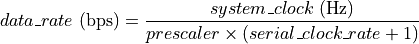
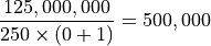
For example, the CowPi_stdio library configures the SPI hardware for 500kbps when the system clock is 125MHz by setting the prescaler to 250 and the serial clock rate to 0:
Controller Output/Peripheral Input Sequence
The typical SPI controller output/peripheral input sequence is:
if necessary, enabling the SPI hardware
signaling the peripheral to receive data by setting the chip select pin to 0
transmitting one or more data bytes
signaling the peripheral to latch the data into its permanent register by setting the chip select pin to 1
if necessary, disabling the SPI hardware
Unlike some other microcontrollers, the RP2040’s SPI hardware controls the chip select pin; the program does not need to do so.
Todo
It does not
Before writing a byte to the cowpi_spi_t’s data field, the program should busy-wait until there is room in the transmit queue (indicated by bit 1 of the cowpi_spi_t’s status field).
The pseudocode for this sequence is:
1(* assume variable spi is a reference to a cowpi_spi_t structure *)
2(* assume variable bit_order indicates whether the peripheral expects MSB first (0) or LSB first (1) *)
3(* assume variable select_pin is an integer identifying the chip select pin *)
if necessary, enable the SPI hardware
4        (* set clock rate 500kHz *)
5spi->prescaler := 250
6        (* Enable SPI, 8-bit data word*)
7spi->control := bitwise_or((1LL << 33), 7)
transmit one or more data bytes:
 8for each byte of data do
 9            (* RP2040 SPI hardware only transmits MSB first, so reverse bits if LSB first is required *)
10    if bit_order = 1 then
11        data_byte := reverse_bits(data_byte)
12            (* make sure the queue isn't full *)
13    busy_wait_while(bit 1 of spi->status = 0)
14            (* send the data that the peripheral needs *)
15    spi->data := data_byte
if necessary, disable the SPI hardware
16        (* make sure all transmissions are complete *)
17busy_wait_while(bit 0 of spi->status = 0)
18        (* Disable SPI *)
19spi->control := 0
Tip
The for each expression in the pseudocode should be understood to be the mathematical  operator.
If there are several bytes that are handled identically, then writing a loop probably makes sense.
On the other hand, if there are a small number of bytes, each of which must be handled differently,
then it probably makes more sense to write straight-line code.
operator.
If there are several bytes that are handled identically, then writing a loop probably makes sense.
On the other hand, if there are a small number of bytes, each of which must be handled differently,
then it probably makes more sense to write straight-line code.
Tip
If you do not need to change the SPI mode or other SPI settings, you do not need to disable the SPI hardware between uses. By choosing to leave the SPI hardware active, the transmit queue can empty while your program takes other actions.
Attention
The specific data byte sequence to be transmitted is described in the Output Devices Section.
Inter-Integrated Circuit Protocol
The RP2040 has two sets of I2C registers. The CowPi_stdio library uses I2C0 to communicate with display modules. If your intended application is simplified by placing peripherals on a separate set of I2C registers, then I2C1 can be exposed through GP18 & GP19 (boosted to 5Von on the Cow Pi mk3c and mk4b) or through GP26 & GP27 (operating at 3.3V on all Pico-based Cow Pi circuits). The registers include:
IC_CONThe I2C Control Register.
IC_SS_SCL_HCNTThe I2C Standard Speed SCL High Count Register.
IC_SS_SCL_LCNTThe I2C Standard Speed SCL Low Count Register.
IC_FS_SCL_HCNTThe I2C Fast Mode SCL High Count Register.
IC_FS_SCL_LCNTThe I2C Fast Mode SCL Low Count Register.
IC_ENABLEThe I2C Enable Register
You do not need to configure I2C0; the CowPi_stdio library takes care of all necessary configuration for controller-transmitter mode at 100kbps.
IC_TARThe I2C Target Address Register. Writing the target peripheral’s address in the
IC_TARregister will cause the microcontroller to transmit a “Start Bit”.IC_SARThe I2C Peripheral Address Register. If the I2C hardware is configured to act as a peripheral, then its address can be set through this register; the default address is 0x55.
IC_DATA_CMDThe I2C Data and Command Register. Write data (or commands) to this register to place them in the transmit queue; Read data from this register to retrieve them from the receive queue.
IC_STATUSThe I2C Status Register. Reading particular bits from the
IC_STATUSregister indicates the status of a data transfer.IC_TXFLRThe I2C Transmit Level Register. This register indicates the number of entries in the transmit queue.
IC_RXFLRThe I2C Receive Level Register. This register indicates the number of entries in the receive queue.
The I2C hardware has four modes of operation: controller transmitter, controller receiver, peripheral transmitter, and peripheral receiver.[1] In the Cow Pi’s typical usage, the controller transmitter mode will be used to drive the display module. For this reason, the discussion in this datasheet will focus on the controller transmitter mode.
The nature of I2C allows for uses other than the display module without compromising the ability to work with the display module. If you choose to expand the Cow Pi in such a manner that other I2C modes are necessary, see Section 4.3 of the RP2040 datasheet for details.
If you use the RP2040 as a peripheral while it is in the Cow Pi circuit, we strongly advise using ICR1 for that purpose.
Structure for Memory-Mapped Input/Output
The CowPi library provides data structures to access the memory-mapped I/O registers in a more readable form.
Specifically, the cowpi_i2c_t structure provides meaningfully-named fields in place of the multi-letter register names.
-
struct cowpi_i2c_t
Structure for the I2C (aka IIC) hardware.
See RP2040 datasheet for configuration and use.
Public Members
-
uint32_t control
I2C control register (IC_CON)
-
uint32_t target_address
I2C target address register (IC_TAR)
-
uint32_t peripheral_address
I2C peripheral address register (IC_SAR)
-
uint32_t __pad0__
padding (apparently unusued address)
-
uint32_t data
I2C data buffer and command register (IC_DATA_CMD)
-
uint32_t __pad1__
padding (unused bits 31..12 of IC_DATA_CMD)
-
uint32_t standard_clock_high_count
I2C standard speed SCL high Count register (IC_SS_SCL_HCNT)
-
uint32_t standard_clock_low_count
I2C standard speed SCL low Count register (IC_SS_SCL_LCNT)
-
uint32_t fast_clock_high_count
I2C fast speed SCL high Count register (IC_FS_SCL_HCNT)
-
uint32_t fast_clock_low_count
I2C fast speed SCL low Count register (IC_FS_SCL_LCNT)
-
uint32_t DO_NOT_TOUCH[0x50]
padding (interrupt-related registers)
-
uint32_t enable
I2C enable register (IC_ENABLE)
-
uint32_t status
I2C status register (IC_STATUS)
-
uint32_t tx_fifo_level
I2C transmit FIFO level register (IC_TXFLR)
-
uint32_t rx_fifo_level
I2C receive FIFO level register (IC_RXFLR)
-
uint32_t control
After you create a pointer to a cowpi_i2c_t structure that points to the lowest-addressed register (I2C0.IC_CON at 0x40044000, or I2C1.IC_CON at 0x40048000, per Table 24).
For example, if we wanted to determine if there is room in the transmit queue, and then enable the I2C hardware as an controller, then we could do so with C code similar to this:
1volatile cowpi_i2c_t *i2c = (cowpi_spi_t *)(0x4003C000);
2uint32_t status = i2c->status & 0x2;    // mask-off the irrelevant bits
3i2c->enable = 1;                        // Enable bit
You may have noticed that this code does not use the read/modify/write pattern. Because of the particular uses of these registers, you may find it easier to explicitly assign each control bit value afresh, rather than modify the pre-existing values.
Status and Data Bits
Table 24 identifies the particular bits in some of the I2C registers.
Register Name |
I2C0 Address
I2C1 Address
|
Bits 31..12 |
Bit 11 |
Bit 10 |
Bit 9 |
Bit 8 |
Bit 7 |
Bit 6 |
Bit 5 |
Bit 4 |
Bit 3 |
Bit 2 |
Bit 1 |
Bit 0 |
|---|---|---|---|---|---|---|---|---|---|---|---|---|---|---|
Control Register
IC_CON
|
0x40044000
0x40084000
|
Unused |
STOP_DET_IF_CONTROLLER_ACTIVE |
RX_FIFO_FULL_HLD_CTRL |
TX_EMPTY_CTRL |
STOP_DET_IFADDRESSED |
IC_PERIPHERAL_DISABLE |
IC_RESTART_EN |
IC_10BITADDR_CONTROLLER |
IC_10BITADDR_PERIPHERAL |
SPEED |
CONTROLLER_MODE |
||
Target Address Register
IC_TAR
|
0x40044004
0x40048004
|
Unused |
SPECIAL |
GC_OR_START |
IC_TAR |
|||||||||
Peripheral Address Register
IC_SAR
|
0x40044008
0x40048008
|
Unused |
IC_SAR |
|||||||||||
Tx/Rx Data Buffer and Command Register
IC_DATA_CMD
|
0x40044010
0x40048010
|
Unused |
FIRST_DATA_BYTE |
RESTART |
STOP |
CMD |
DAT |
|||||||
Enable Register
IC_ENABLE
|
0x4004406C
0x4004806C
|
Unused |
TX_CMD_BLOCK |
ABORT |
ENABLE |
|||||||||
Status Register
IC_STATUS
|
0x40044070
0x40048070
|
Unused |
PERIPHERAL_ACTIVITY |
CONTROLLER_ACTIVITY |
RFF |
RFNE |
TFE |
TFNF |
ACTIVITY |
|||||
The CowPi_stdio library configures the I2C0 hardware to transmit at 100kbps. In this section we focus on the needs of the application programmer working with a display module connected to I2C0 and shall describe only the status and data bits. If you need information about the setting the bit rate, addressing a target peripheral, configuring the peripheral address, or shutting down and enabling the I2C hardware, see Section 4.3.2 of the RP2040 datasheet for the bit descriptions.
Data Bits
The eight data bits are straight-forward.
When in controller transmitter mode, place the byte that needs to be transmitted into the Data Register (or the data field of a cowpi_i2c_t variable);
there is generally no need to use the distinct bits.
Similarly, when in controller receiver mode, the head of the receive queue can be found by reading from the Data Register.
Bits 11..8 have particular uses. Most significantly, the last data byte placed into the transmit queue should be bitwise-ORed with a 1 in bit 9, to instruct the I2C hardware to transmit a STOP bit.
Status Bits
There are seven bits in the SPI Status Register that allow a program to learn when it is safe to control the hardware.
- Bit 6, Peripheral FSM Activity Status
- Bit 5, Controller FSM Activity Status
The I2C hardware sets an FSM Activity Status flag to 1 when the corresponding FSM is busy.
- Bit 4, Receive FIFO Full
The I2C hardware sets this flag to 1 when the receive queue is full, and clears it to 0 when there is room to receive another data word.
- Bit 3, Receive FIFO Not Empty
The I2C hardware clears this flag to 0 when the receive queue is empty, and sets it to 1 when there is at least one data word in the queue.
If and only if this bit is 1, then there is data that can be read from the Data Register.
- Bit 2, Transmit FIFO Empty
The I2C hardware sets this flag to 1 when the transmit queue is empty, and clears it to 0 when there is at least one data word in the queue.
- Bit 1, Transmit FIFO Not Full
The I2C hardware clears this flag to 0 when the transmit queue is full, and sets it to 1 when there is room for at least one data word in the queue.
If and only if this bit is 1, then it is safe to write data to the Data Register.
- Bit 0, Activity Flag
The I2C hardware sets this flag to 1 when it is transmitting or receiving, and clears it to 0 when the I2C hardware is idle.
Controller Transmitter Sequence
Generally speaking, the I2C controller transmitter sequence consists of:
contacting the peripheral by transmitting a start bit followed by the desired peripheral’s address
transmitting one or more data bytes
transmitting a stop bit
Before writing a byte to the cowpi_i2c_t’s data field, the program should busy-wait until there is room in the transmit queue (indicated by bit 1 of the cowpi_i2c_t’s status field).
To transmit the STOP bit, the last byte placed in the transmit queue should be bitwise-ORed with a 1 in bit 9!
The pseudocode for this sequence is:
1(* assume variable i2c is a reference to a cowpi_i2c_t structure *)
contact the peripheral by transmitting a start bit followed by the desired peripheral’s address
2        (* "To generate a START BYTE, the CPU needs to write only once into these bits." *)
3i2c->target_address := peripheral_address
transmit one or more data bytes
 4        (* send the data that the peripheral needs *)
 5for each byte of data do
 6            (* determine whether the stop bit should be queued *)
 7    if data_byte is the last byte then
 8        stop_bit := 1 << 9
 9    else
10        stop bit := 0
11            (* make sure the queue isn't full *)
12    busy_wait_while(bit 1 of i2c->status = 0)
13            (* send the data that the peripheral needs *)
14    i2c->data := bitwise_or(data_byte, stop_bit)
transmit a stop bit
15        (* the stop bit is in the queue; we just need to wait for it to be transmitted *)
16busy_wait_while(bit 2 of i2c->status = 0)
Tip
The for each expression in the pseudocode should be understood to be the mathematical operator.
If there are several bytes that are handled identically, then writing a loop probably makes sense.
On the other hand, if there are a small number of bytes, each of which must be handled differently,
then it probably makes more sense to write straight-line code.
Attention
The specific data byte sequence to be transmitted is described in the Output Devices Section.
Interrupts
Most interrupts on the RP2040 are handled by registering specific functions as interrupt service routines (ISRs).
Neither the official Arduino core for the RP2040, nor MBED OS on which it is built, offer a low-level mechanism similar to AVR-libc’s ISR() macro to do this.
(The Raspberry Pi Pico SDK, and the unofficial Arduino-Pico core on which it is built, however, do.)
Instead, in the specific case of pin-based interrupts, we normally would be expected to use the Arduino attachInterrupt() function function when using the Arduino toolchain,
or the gpio_set_irq_enabled_with_callback() function when using the Raspberry Pi Pico SDK.
However, we very strongly recommend using the CowPi library’s :func:`cowpi_register_pin_ISR` function for increased portability across microcontrollers and across toolchains.
Timers
The RP2040 has a single general-purpose system timer and a small handful of specialized timers. As with the other I/O registers, the registers used by these timers are mapped into the data memory address space.
For now, we will focus on the general-purpose timer (RP2040 datasheet, §4.6).
Structure for Memory-Mapped Timer Registers
The CowPi library provides a data structure for the 64-bit timer, allowing access to the memory-mapped timer registers in a more readable form.
The registers can be access by creating pointer a to 0x40054000.
-
struct cowpi_timer_t
Structure to access the global microsecond timebase.
There is a single 64-bit time counter that increments every microsecond. The 64-bit value can safely be assumed to never overflow unless you expect your system to run for more than 584.5 thousand years. The lower 32 bits, however, will overflow after about 71.6 minutes. Reading from
lower_wordfirst will simultaneously latch the upper 32 bits intoupper_word, guaranteeing a consistent 64-bit value.Reading from
raw_lower_wordandraw_upper_worddoes not offer this behavior.Public Members
-
uint32_t __pad0__
padding (write upper word)
-
uint32_t __pad1__
padding (write lower word)
-
uint32_t upper_word
Bits 63..32 of time (always read lower_word before upper_word)
-
uint32_t lower_word
Bits 31..0 of time (always read lower_word before upper_word)
-
uint32_t alarms[4]
Alarm will fire when lower_word == alarms[n].
-
uint32_t alarm_status
Indicates whether alarm[n] is armed; also use to disarm alarm[n].
-
uint32_t raw_upper_word
Bits 63..32 of time that can be read without side effects.
-
uint32_t raw_lower_word
Bits 31..0 of time that can be read without side effects.
-
uint32_t __pad2__
padding (debug pause)
-
uint32_t pause
Use to pause the counter.
-
uint32_t __pad0__
Todo
bare-metal alarm interrupts
Caution
The RP2040 provides registers that permit an application programmer to change the timer’s counter. The structure provided by the CowPi library does not expose these registers, replacing their addresses in the structure with padding. This is because nearly every framework assumes monotonically-increasing time.
The seven fields in the structure are:
upper_wordlower_wordUpper and lower 32-bit words of the 64-bit counter; these fields should be read if the application requires consistent time while running for more than an hour
alarmsAn array of four alarms; an alarm will trigger an interrupt when the counter’s lower word matches the corresponding alarm register. Writing a value to an alarm register will set the corresponding bit in
alarm_statusalarm_statusIndicates whether a particular alarm is armed (1) or not (0). A pending alarm can be cancelled by writing a 0 to the corresponding bit.
raw_upper_wordraw_lower_wordUpper and lower 32-bit words of the 64-bit counter; these fields should be read when no side-effects are desired and consistency between the upper and lower words is immaterial.
pauseSet high to pause the timer.
Reading the Timer Counter
The timer increments its counter once per microsecond. Thus, assuming the timer is never paused, the 64-bit counter contains the number of microseconds since the system was powered-up.
Reading the 64-bit Counter
The 64-bit counter cannot overflow during the span of a typical academic term:

However, the RP2040 has a 32-bit data bus and cannot read the full 64 bits from the counter in a single cycle; instead, the upper and lower word are accessed separately. The 32-bit lower word can overflow during the span of a typical lab period:

Unless otherwise anticipated, if the lower word happens to overflow between reading one of the counter’s words and reading the other word,
then the upper and lower words will be inconsistent: depending on which word is read first, the measured time will either be fast or slow by about  minutes.
To address this, whenever a program reads from lower_word, the consistent upper word is latched so that it is available to be read from upper_word in the next cycle.
Note
This latching occurs only if the lower word is read first
The pseudocode to obtain the full 64-bit counter is thus:
1        (* assume variable timer is a reference to a cowpi_timer_t structure at 0x40054000 *)
2lower_32bits = timer->lower_word
3upper_32bits = timer->upper_word
4counter_64bits = bitwise_or((uint64_t)upper_32bits << 32, lower_32_bits)
Note
The preceding pseudocode has a race condition if two processes (or threads) attempt to read the timer concurrently.
Note
The C standard does not specify the evaluation order of the sub-expressions in a bitwise-OR expression. We recommend that you explicitly read the lower word first to ensure that it is, in fact, read before the upper word.
Reading a 32-bit Counter
If you are not concerned about the possibility of overflow every minutes, then you can read from raw_upper_word and raw_lower_word.
If you only need a 32-bit microsecond counter, then reading from raw_lower_word will provide you with the number of microseconds since power-up, modulo  .
.
5counter_32bits = timer->raw_lower_word;
A somewhat less likely scenario can make use of the raw_upper_word:
Because the lower word overflows every microseconds, the upper word increments approximately once every  .
.
6days_since_powerup = timer->raw_upper_word / 20;
7        (* has error of about 3 minutes per day *)
Note
There are no race conditions inherent in two processes (or threads) reading the “raw” timer words concurrently.
Scheduling Alarms
We advise against directly accessing the alarm registers while using the official Arduino toolchain, which is based on the Mbed OS,
as it is not clear how the Mbed OS uses the alarms.
If you do not use CowPi functions () to manage timer interrupts, then
we recommend instead using the Mbed OS Ticker and Timeout APIs.
Todo
Watchdog Timer
Todo
Real-Time Clock
Todo
PWM
Todo
ADC
Todo
Temperature
Probably as an “Extension Option”
Todo
UART
Bare-Metal Concurrency
This is a placeholder section. Currently the only toolchain for RP2040 that the CowPi library supports is the official Arduino toolchain, built on top of Mbed OS.
Warning
For the time being, we advise against using the memory-mapped communication & synchronization registers, as the official Arduino toolchain does not support dual-core operation, and it is not clear which (if any) of the spinlocks are used by Mbed OS and would require deconfliction with application code.
Structure for Memory-Mapped Interprocess Communication & Synchronization Registers
-
struct cowpi_concurrency_t
Structure to coordinate concurrent behavior between the two cores.
A 32 bit wide, 8 word deep FIFO pipe can be used to pass data/messages between the cores.
- Todo:
incorporate interrupts
Public Members
-
uint32_t pipe_status
FIFO Status register; see datasheet for bit descriptions.
-
uint32_t pipe_write
Write word in this field to send message to other core.
-
uint32_t pipe_read
Read word from this field to obtain message from other core.
-
uint32_t spinlock_status
Status of each of the 32 mutex tokens (1=locked, 0=unlocked)
-
uint32_t DO_NOT_TOUCH_1[0x20]
padding (divider)
-
uint32_t DO_NOT_TOUCH_2[0x80]
padding (interpolators)
-
uint32_t spinlocks[32]
Busy-wait until reading produces non-zero value; write to release (see datasheet)